- A Bluetooth low-energy (BLE) transceiver with TX/RX switchable on-chip matching network, 2.75mW high-IF discrete-time receiver, and 3.6mW all-digital transmitter
- Conference
- Keywords
- Access to Document
- Fingerprint
- Cite this
- Bluetooth Low Energy
- 4th generation multiprotocol SoC
- Meet nRF54H20!
- Best-in-class Bluetooth Low Energy SoCs
- Bluetooth Low Energy flagship SoC
- Supports an extensive range of wireless protocols
- nRF52 Series
- All-flash based SoCs
- Tokyo Tech slashes power consumption in Bluetooth Low-Energy transceiver by more than half
- Why BLE matters
- Key features
- Looking ahead
A Bluetooth low-energy (BLE) transceiver with TX/RX switchable on-chip matching network, 2.75mW high-IF discrete-time receiver, and 3.6mW all-digital transmitter
We present a new ultra-low-power (ULP) transceiver for Internet-of-Things (IoT) optimized for 28-nm CMOS. The receiver (RX) employs a high-rate (up to 10 GS/s) discrete-time (DT) architecture with intermediate frequency (IF) placed beyond the 1/f noise corner of MOS devices. New multistage multi-rate charge-sharing bandpass filters are adapted to achieve high out-of-band linearity, low noise and low power consumption. A transmitter (TX) employs an all-digital PLL (ADPLL) with switched-current-source digitally controlled oscillator (DCO) and switching PA. An integrated on-chip matching network serves both PA and LNTA, thus allowing a 1-pin direct antenna connection with no external antenna filters. The transceiver consumes 2.75mW in RX and 3.6mW in TX when delivering 0 dBm in Bluetooth LE.
Conference
| Conference | 30th IEEE Symposium on VLSI Circuits, VLSI Circuits 2016 |
|---|---|
| Country/Territory | United States |
| City | Honolulu |
| Period | 14/06/16 → 17/06/16 |
Keywords
- Bluetooth
- Internet of Things
- MOS integrated circuits
- band-pass filters
- oscillators
- phase locked loops
- radio transceivers
- radio transmitters
- 1-pin direct antenna connection
- Bluetooth LE
- Bluetooth low-energy transceiver
- CMOS
- Internet-of-Things
- IoT
- MOS devices
- TX/RX switchable on-chip matching network
- The receiver
- all-digital PLL
- all-digital transmitter
- discrete-time architecture
- high-IF discrete-time receiver
- integrated on-chip matching network
- multirate charge-sharing bandpass filters
- power 2.75 mW
- power 3.6 mW
- power consumption
- size 28 nm
- switched-current-source digitally controlled oscillator
- transmitter
- ultra-low-power transceiver
- Band-pass filters
- Capacitors
- Gain
- Power demand
- Switches
- System-on-chip
- Transceivers
Access to Document
Fingerprint
Dive into the research topics of ‘A Bluetooth low-energy (BLE) transceiver with TX/RX switchable on-chip matching network, 2.75mW high-IF discrete-time receiver, and 3.6mW all-digital transmitter’. Together they form a unique fingerprint.
Cite this
- APA
- Author
- BIBTEX
- Harvard
- Standard
- RIS
- Vancouver
title = «A Bluetooth low-energy (BLE) transceiver with TX/RX switchable on-chip matching network, 2.75mW high-IF discrete-time receiver, and 3.6mW all-digital transmitter»,
abstract = «We present a new ultra-low-power (ULP) transceiver for Internet-of-Things (IoT) optimized for 28-nm CMOS. The receiver (RX) employs a high-rate (up to 10 GS/s) discrete-time (DT) architecture with intermediate frequency (IF) placed beyond the 1/f noise corner of MOS devices. New multistage multi-rate charge-sharing bandpass filters are adapted to achieve high out-of-band linearity, low noise and low power consumption. A transmitter (TX) employs an all-digital PLL (ADPLL) with switched-current-source digitally controlled oscillator (DCO) and switching PA. An integrated on-chip matching network serves both PA and LNTA, thus allowing a 1-pin direct antenna connection with no external antenna filters. The transceiver consumes 2.75mW in RX and 3.6mW in TX when delivering 0 dBm in Bluetooth LE.»,
keywords = «Bluetooth, Internet of Things, MOS integrated circuits, band-pass filters, oscillators, phase locked loops, radio transceivers, radio transmitters, 1-pin direct antenna connection, Bluetooth LE, Bluetooth low-energy transceiver, CMOS, Internet-of-Things, IoT, MOS devices, TX/RX switchable on-chip matching network, The receiver, all-digital PLL, all-digital transmitter, discrete-time architecture, high-IF discrete-time receiver, integrated on-chip matching network, multirate charge-sharing bandpass filters, power 2.75 mW, power 3.6 mW, power consumption, size 28 nm, switched-current-source digitally controlled oscillator, transmitter, ultra-low-power transceiver, Band-pass filters, Capacitors, Gain, Power demand, Switches, System-on-chip, Transceivers»,
author = «Kuo,
Bluetooth Low Energy
If you want to add Bluetooth Low Energy connectivity to your product, you have come to right place. We offer a broad portfolio of wireless multiprotocol System-on-Chips (SoCs). All our SoCs are extremely advanced and power efficient, but have different feature sets and memory configurations. We ship more than 1 million Bluetooth LE SoCs every day and in 2022 alone our customers certified 446 new end-products, making us the market leader (39 % market share). Our customers select us because we offer high quality SoCs with ultra-low power consumption, protocol stacks with excellent interoperability and easy-to-use software and tools. In addition, we offer free technical support for anyone, guiding you through the whole product development process.
Explore our Bluetooth Low Energy solutions below!
4th generation multiprotocol SoC
Meet nRF54H20!
nRF54H20 offers s uperior processing power, a generous amount of memory, best-in-class radio, and state-of-the-art security, all integrated into a compact ultra-low power SoC.
Best-in-class Bluetooth Low Energy SoCs
Bluetooth Low Energy flagship SoC
The nRF5340 SoC is our Bluetooth Low Energy flagship. It is the first SoC in the nRF53 Series and is the world’s first wireless SoC with two Arm® Cortex®-M33 processors. The combination of two flexible processors and the advanced feature set make it the ideal choice for LE Audio, advanced wearables, and other complex IoT applications. The nRF5340 is an all-in-one SoC, including a superset of the most prominent nRF52® Series features. Features like Bluetooth® 5.4, high-speed SPI, QSPI, USB, up to 105 °C operating temperature, and more, are combined with more performance, memory and integration, while minimizing current consumption. It also offers security features such as trusted execution, root-of-trust and secure key storage.
Supports an extensive range of wireless protocols
The nRF5340 is a Bluetooth 5.4 SoC and is capable of taking all angle-of-arrival (AoA) and angle-of-departure roles (AoD) in Bluetooth Direction Finding. It also supports LE Audio, Long Range, high-throughput 2 Mbps and Advertising Extensions features. Mesh protocols like Bluetooth mesh, Thread and Zigbee can be run concurrently with Bluetooth Low Energy, enabling smartphones to provision, commission, configure and control mesh nodes. NFC, ANT, 802.15.4 and 2.4 GHz proprietary protocols are also supported.
nRF52 Series
The nRF52 Series consists of seven multiprotocol Bluetooth 5.4 SoCs that integrate a powerful yet efficient 64 MHz Arm Cortex-M4 CPU. Flash memory range from 192 KB to 1024 KB while RAM range from 24 KB to 256 KB. The nRF52 Series offers simpler cost-effective options and highly-advanced options, all with ultra-low power consumption. The nRF52 Series is truly the ideal platform for basing a product portfolio upon. The similar hardware and software architecture results in excellent software portability, increasing software reusability and lowering time-to-market and development cost.
All-flash based SoCs
The nRF52 and nRF53 Series are all-flash based SoCs. Flash memory brings complete flexibility and upgradability to your products. They can be re-programmed in the factory or in the field with over-the-air device firmware upgrades (OTA DFU). This enables product updates and feature additions any time, anywhere.
Tokyo Tech slashes power consumption in Bluetooth Low-Energy transceiver by more than half
![]()
Researchers at Tokyo Institute of Technology (Tokyo Tech) announce a Bluetooth Low-Energy transceiver with the lowest ever power consumption — a breakthrough set to accelerate widespread adoption of Internet of Things (IoT) applications in Japan and around the globe.
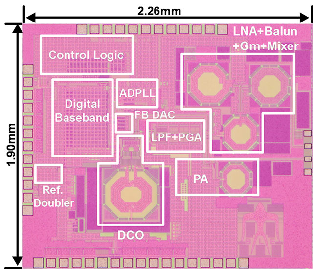
Figure. A photograph of the chip
The chip was designed using standard 65-nanometer CMOS technology.
An ultra-low-power Bluetooth Low-Energy transceiver designed for use in the popular 2.4 GHz band has been developed by a group of researchers led by Kenichi Okada of Tokyo Institute of Technology, Japan.
When transmitting, the transceiver consumes 2.9 milliwatts (mW) and when receiving, it consumes just 2.3 mW. Given that minimizing power consumption is a requirement for the oncoming IoT era, these figures are remarkable, as they represent less than half the power consumed by previous transceivers (see Table).
Table. A performance comparison of BLE transceivers
Tokyo Tech’s BLE transceiver achieves a dramatic reduction in power consumption — down to less than half of those previously reported. All figures are in milliwatts (mW).
Why BLE matters
Within the next decade, IoT is projected to become a multi-trillion US dollar industry. Bluetooth Low-Energy (BLE) is in the spotlight as a key technology spurring the growth of this fast-evolving market. Already embedded in millions of Apple and Android devices, BLE is the most used short-range wireless technology aimed at low-power and low-cost connectivity.
Low-energy solutions are in demand not only for smartphones and watches, but also for emerging applications in the medical and healthcare fields, factories and public infrastructure such as roads, bridges and tunnels. IoT sensors for early detection and warning systems could mean the difference between life and death.
«Our research grew out of this need for connectivity,» explains Okada. «In an IoT world, trillions of devices will be used. To extend battery life and aim for maintenance-free operations, reducing power consumption is vital.»
Key features
The BLE transceiver has excellent receiver sensitivity 1 and high interference tolerance 2 , while also realizing the lowest power consumption.
The transmitter employs an all-digital phase-locked loop (ADPLL), an attractive building block for BLE, as it is less susceptible to noise compared to its analog counterpart. The transceiver was designed in a 65-nanometer CMOS process 3 .
In another study focusing on ADPLL, the researchers achieved a figure of merit (FoM) 4 of -246 dB, one of the best obtained so far. The FoM is an important metric for evaluating the trade-off between performance and power consumption.
The above results arose from a project supported by Japan’s New Energy and Industrial Technology Development Organization (NEDO).
Looking ahead
In future, Okada says: «The PLL could operate on just 0.65 mW, and studies are underway to reduce our transceiver’s power consumption even further.»
The team will present their findings at the 2018 International Solid-State Circuits Conference (ISSCC). Held every February in San Francisco, the conference, popularly known as the Chip Olympics, is regarded as the leading forum on integrated circuit research and development.
A measure of how well a receiver can pick up the tiniest of signals. The figure reached in this study was an impressive -94 decibels relative to 1 milliwatt (dBm).
Referring to the need for high tolerance to interference from other signals operating in the busy 2.4 GHz band.
A standard method of building integrated circuits using silicon-based complementary metal–oxide–semiconductor (CMOS) technology.
The FoM evaluates the trade-off between jitter (related to noise in wireless communication) and power consumption. Reducing jitter is desirable for improving the quality of communication, but this requires more energy, so there is a trade-off between performance and power consumption. In general, the lower the FoM, the better. The figure of -246 dB is one of the lowest ever achieved.
A 0.98 mW Fractional-N ADPLL Using 10b Isolated Constant-Slope DTC with FOM of -246 dB for IoT Applications in 65 nm
Session 15, RF PLLs, 2018 IEEE International Solid-State Circuits Conference
Hanli Liu, Zheng Sun, Dexian Tang, Hongye Huang, Tohru Kaneko, Wei Deng, Rui Wu, Kenichi Okada, Akira Matsuzawa
An ADPLL-Centric Bluetooth Low-Energy Transceiver with 2.3 mW Interference-Tolerant Hybrid-Loop Receiver and 2.9 mW Single-Point Polar Transmitter in 65 nm CMOS
Session 28, Wireless Connectivity, 2018 IEEE International Solid-State Circuits Conference

School of Engineering
—Creating New Industries and Advancing Civilization—
Information on School of Engineering inaugurated in April 2016
Associate Professor Kenichi Okada
School of Engineering, Tokyo Institute of Technology
Public Relations Section, Tokyo Institute of Technology