- High-gain 2.4 GHz PCB Wifi Antenna
- Description
- What is High-gain 2.4 GHz PCB Wifi Antenna?
- PCB Wifi Antenna Description and features
- High-gain 2.4 GHz PCB Wifi Antenna Specifications
- High-gain 2.4 GHz Wifi PCB Antenna Electrical Specifications
- High-gain 2.4 GHz Wifi PCB Antenna Mechanical Specifications
- Embedded Antenna High-gain 2.4 GHz PCB Antenna Features
- Reviews
- 2.4GHz 5GHz PCB Wifi Antenna Design
- Description
- Who Supplies PCB Wifi Antenna Design?
- PCB Wifi Antenna Design small antenna design in portable wireless products
- PCB Wifi Antenna Design Features
- Reviews
High-gain 2.4 GHz PCB Wifi Antenna
C&T RF Antennas Inc provides the High-gain 2.4 GHz PCB Wifi antenna design & products, or other frequency antennas, etc.
Contact the C&T RF sales team for more High-gain 2.4 GHz wifi PCB antenna details or other antenna types.
Description
What is High-gain 2.4 GHz PCB Wifi Antenna?
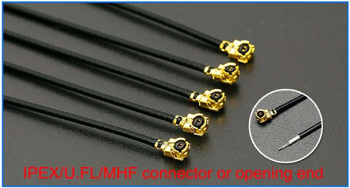
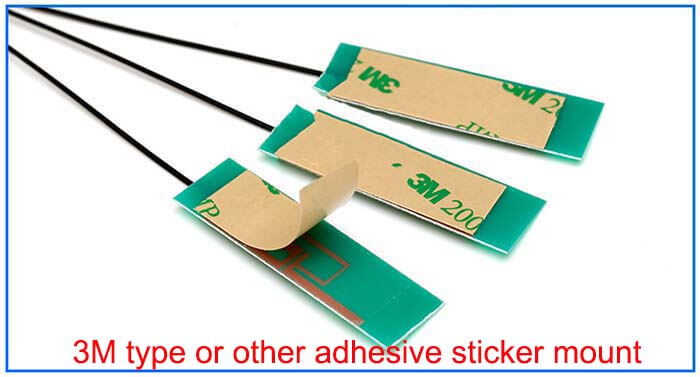
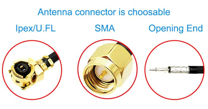
The PCB Wifi Antenna 2.4 GHz High-gain Antenna CTRF-ANTENNA-PCB-2450-5826-IPEX comes with a 6dBi high-gain antenna design, self-adhesive sticker for an easy mount, and Ipex/U.FL connector, suitable for every wifi application device wifi antenna manufactured by C&T RF Antennas Inc.
PCB Wifi Antenna Description and features
The antenna portfolio according to proven standards is part of the overall wireless LAN solution.
Combinations with cabling technology and mounting accessories wifi devices. Variety of applications. Robust and certified. Easy assembly. Reliable connection.
The High-gain 2.4 GHz PCB antenna is manufactured by C&T RF Antennas Inc. The high-gain & high-performance wifi antenna 2.4 GHz antenna manufacturer in China.
C&T RF Antennas Inc provides the RF wireless antennas with PCB & Flex PCB & Omni antenna types, covering the below frequencies:
Contact us for more information on the High-gain 2.4 GHz wifi PCB antenna such as High-gain 2.4 GHz PCB Wifi Antenna datasheet, High-gain 2.4 GHz PCB Wifi Antenna pricing, and High-gain 2.4 GHz PCB Wifi Antenna inventory.
Or other High-gain 2.4 GHz PCB Wifi Antenna styles.
High-gain 2.4 GHz PCB Wifi Antenna Specifications
High-gain 2.4 GHz Wifi PCB Antenna Electrical Specifications
High-gain 2.4 GHz Wifi PCB Antenna Mechanical Specifications
Embedded Antenna High-gain 2.4 GHz PCB Antenna Features

Reviews
You must be logged in to post a review.
2.4GHz 5GHz PCB Wifi Antenna Design
C&T RF Antennas Inc is the embedded antenna PCB Wifi Antenna Design & Antenna manufacturer in China. We provide the RF antenna design with other antenna radio frequencies.
Contact us for more PCB wifi antenna design details.
Description
Who Supplies PCB Wifi Antenna Design?
C&T RF Antennas Inc supplies the single-band 2.4GHz PCB Wifi Antenna Design, single-band 5.8GHz PCB Wifi Antenna Design, dual-band PCB wifi antenna design, flexible PCB wifi antenna design with single-band & dual-band, etc.
Besides the PCB Wifi Antenna Design, we also have the 4G LTE PCB Antenna Design and 4G LTE Antenna Design FPC Antenna Design for your choice.
C&T RF Antennas Inc provides telecommunication antennas with the antenna radio frequencies such as 169MHz, 230MHz, 315MHz, 433MHz, 868MHz, 915MHz, Lora, VHF&UHF, NB-IoT, GSM, Wifi 2.4GHz, 5.8GHz, 2G 3G 4G LTE, GPS, 5G NR, UWB, etc.
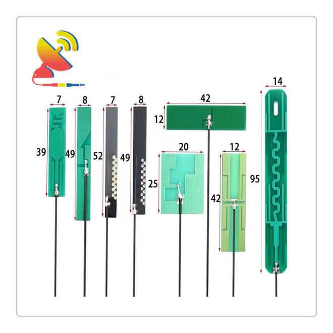
Below are the single-band PCB Wifi Antenna Designed styles:
Below are the existing dual-band PCB Wifi Antenna Design styles for your choice.
Below are the existing Flexible antenna single-band PCB Wifi Antenna Design and Flexible antenna dual-band PCB Wifi Antenna Design styles for your choice.
PCB Wifi Antenna Design small antenna design in portable wireless products
The loop antenna is easy to implement. The rectangular block antenna uses well-planned PCB space (it can also be a discrete device)
The rectangular block antenna is a wider microstrip transmission line whose length is half of the operating wavelength in terms of electrical characteristics.
The wavelength is not calculated by propagation in a vacuum, but by the insulating PCB material. The resonance frequency of the rectangular block is quite narrow, so its working bandwidth is also quite narrow-about 5% of the nominal center frequency.
Whether this characteristic is good or bad depends on the specific application.
All three types of antennas can be implemented with PCBs, and a multilayer PCB can provide multiple design options, including the ground plane required for certain structures.
This kind of antenna design is used in applications such as remote unlocking (RKE) and garage openers that are not demanding performance.
Since the design cost of the PCB antenna is negligible, when and what makes it not a design priority? Several of the dominant factors are related to front-end design and actual implementation.
First, the antenna design is not simple. Even with modeling programs like Numerical Electromagnetic Code, circuit or system engineers are unfamiliar with the electromagnetic world. They are facing a world of electromagnetic fields, not specific voltage and current points or electron currents flowing in a fixed loop.
Secondly, like many engineering designs, competing and conflicting properties such as center frequency, bandwidth, field mode, efficiency, and lobe and gain make it difficult to balance them.
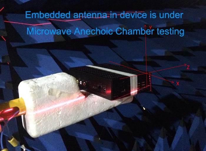
Third, it is not easy to evaluate the performance of an antenna. It requires special test equipment, a non-reflective chamber, or an open area. It also requires time, money, and expertise.
In addition, when evaluating the impact of the user’s hand on the antenna, or vice versa, when evaluating the impact of antenna radiation on the user’s hand, correct test settings must be performed, including the physical copy of the human hand and head.
And these are all theoretical. In fact, there are other factors at play. The antenna certainly occupies the PCB space, and its performance attributes are significantly affected by nearby components and the user’s hands, head, and body.
The relative dielectric constant of human tissue is 40, and the dielectric constant of PCB components is about 25 to 85, so human tissue will excite resonance elements and affect the magnetic field.
In addition, when multiple antennas are required for multi-band operation or shape diversity design, the interaction between several PCB antennas and between antennas and nearby areas will make performance prediction very difficult, and they are sensitive to subtle layout changes.
But some rules constrain the antenna field-specific absorption rate (SAR). SAR is the ratio of mass (human tissue in this case) to the ability to absorb RF;
It is usually measured in two ways:
One is to measure the temperature rise caused by absorption;
The second is to measure the electric field of the fluid that simulates human tissue.
There is more information on the Federal Communications Commission (FCC) website. The near-field and far-field performance of the antenna must be understood and analyzed, and they may be closely related.
Finally, the antenna is not isolated from the front end of the wireless device or the transmit power amplifier stage. The circuit designer must determine the impedance of the antenna and associated stages, and then design a matching network to maximize power transfer across the target bandwidth.
The antenna subsystem includes a front-end receiving amplifier or transmitting amplifier, a matching network, and the antenna itself.
This is usually a difficult design task, involving professional calculations and measurements, and special tools, such as the Smith chart.
PCB Wifi Antenna Design Features